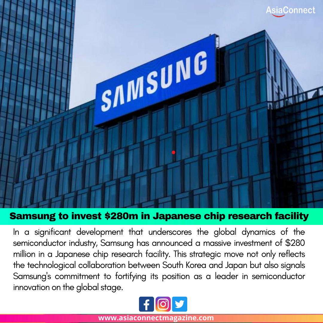
In a significant development that underscores the global dynamics of the semiconductor industry, Samsung has announced a massive investment of $280 million in a Japanese chip research facility. This strategic move not only reflects the technological collaboration between South Korea and Japan but also signals Samsung’s commitment to fortifying its position as a leader in semiconductor innovation on the global stage.
Strengthening Technological Alliances
Samsung’s decision to invest in a Japanese chip research facility highlights the importance of cross-border collaborations in the semiconductor industry. Japan, renowned for its technological prowess, has long been a hub for cutting-edge research and development in the field. Samsung’s substantial investment signifies the recognition of Japan’s role in advancing semiconductor technologies.
The move also comes at a time when the semiconductor industry is experiencing heightened global competition, and companies are actively seeking partnerships and collaborations to stay ahead in the rapidly evolving landscape.
Focused Research and Development
The $280 million investment is earmarked for the research and development (R&D) activities of the Japanese chip facility. This allocation underscores Samsung’s commitment to pushing the boundaries of semiconductor technology. R&D investments are pivotal in fueling innovation, driving the development of next-generation chips, and maintaining a competitive edge in the market.
By strategically placing funds into research initiatives, Samsung aims to harness the collective expertise of Japanese researchers and engineers, fostering an environment conducive to breakthroughs in semiconductor design and manufacturing.
Addressing Supply Chain Challenges
The semiconductor industry has been grappling with supply chain challenges, with fluctuations in demand and disruptions to the global supply chain affecting production. Samsung’s investment in a Japanese facility can be viewed as a proactive measure to diversify its manufacturing capabilities and mitigate potential risks associated with a centralized supply chain.
By establishing a stronger presence in Japan, Samsung not only taps into the country’s technological resources but also strategically positions itself to navigate supply chain uncertainties more effectively.
Global Impact on the Semiconductor Landscape
Samsung’s investment sends ripples across the global semiconductor landscape, reinforcing the industry’s interconnected nature. The collaboration between a South Korean tech giant and a Japanese research facility has the potential to set new benchmarks in semiconductor innovation, with implications for a wide range of applications, from consumer electronics to emerging technologies like artificial intelligence and the Internet of Things (IoT).
As the semiconductor market continues to evolve, collaborations between major players become increasingly crucial to drive advancements that shape the future of technology.
Economic and Diplomatic Dimensions
Beyond the technological aspects, Samsung’s investment in a Japanese chip research facility also holds economic and diplomatic significance. It fosters stronger ties between South Korea and Japan in the realm of technology, potentially paving the way for more extensive collaborations in the future.
In an era where geopolitical dynamics often influence business decisions, this investment showcases the potential for mutually beneficial partnerships that transcend political boundaries.
Conclusion
Samsung’s $280 million investment in a Japanese chip research facility marks a strategic move that goes beyond financial considerations. It signifies a commitment to technological innovation, a proactive response to supply chain challenges, and a testament to the importance of global collaborations in the semiconductor industry. As the ripple effects of this investment extend across borders, the semiconductor landscape stands to benefit from the combined expertise of two technological powerhouses, setting the stage for transformative advancements in the field.


